real structures of solids and interfaces
Real crystalline materials contain defects which disturb the periodic arrangement of the atoms in the crystal lattice. In many cases crystal defects determine the properties of the material such as mechanical, optical and electrical. For instance the properties of silicon used for semiconductor technology are determined by defects brought into the crystal by doping with other elements, and the properties can be tailored. Classical diffraction methods yield information on the bulk structure, however, the defect structure of solids remains hidden. Electron microscopy offers the possibility to characterise microscopic defect structures in crystals, and it is the only method available for this task.
The defects are classified according to their size and their dimension, respectively. Point defects (zero dimensional) such as vacancies and interstitial atoms are atomically small. They can not e imaged directly, however lattice relaxations caused by the defects can be studied by diffraction methods. Dislocations are the typical representative of line defects (one dimensional) and exist in virtually all crystals. The periodic arrangement of the crystal is substantially disturbed at a dislocation line and the lattice is strained around the dislocation core. The lattice strain can be made visible in the diffraction contrast of electron microscope images, and the visibility criteria allow to distinguish the various types of dislocations. Edge dislocations in crystals can be directly imaged and analysed by high resolution TEM (HRTEM).
Planar defects (interfaces, two dimensional) may exist within crystals e.g. stacking faults and domain boundaries. In polycrystalline material neighbouring crystallites (grains) with differing orientation are separated by grain boundaries, and in composites and materials systems such as thin films on substrates, interfaces between different phases (phase boundaries) occur. The structure of interfaces is not known a priori. Studies by high resolution TEM are most important and it represents the only method available to obtain detailed structural information on such two dimensional objects.
Interface research of our group currently focuses on the characterisation of twin boundaries and inversion domain boundaries in doped zinc oxide. Zinc oxide (ZnO) is a functional ceramic mainly applied in varistor technology. Varistors are electronic components which efficiently protect electrical systems from voltage spikes without being destroyed themselves. The word "varistor" is artificial, made up from "variable" and "resistor". The properties of varistors are due to an extremely non-linear current-voltage characteristic, the origin of which lies in the microstructure of the material.
Doping of ZnO with oxides of trivalent metals results in characteristic microstructures. The origin for the structures and their development is not yet known. We study as kind of model systems ZnO-Ga2O3, ZnO-Fe2O3, ZnO-In2O3 as well as ZnO-Ga2O3-Bi2O3, ZnO-Fe2O3-Bi2O3. In all these systems twin and inversion structures are observed, i.e. crystal domains develop which are related either by a mirror operation at distinct crystallographic planes (twins) or by an orientation inversion of the ZnO crystal (inversion domain boundary). Twins, domains and the respective interfaces are investigated using the methods of electron diffraction, EDX, electron spectroscopy, energy-filtered TEM and HRTEM. Furthermore, thermodynamic aspects and kinetics of the transport of the added metallic cations are studied in detail.

Inversion domain boundaries (IDBs) in ZnO doped with Fe2O3. Annular dark-field (ADF) STEM image (left) and corresponding Fe map by X-rays (SIX) (middle) show decoration of IDBs with Fe. Atomic resolution ADF image (right) with metal atom positions and model of the boundary structure with a monolayer of Fe3+.
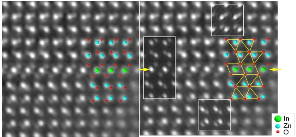
Atomic resolution phase contrast image of an inversion domain boundary (arrows) in ZnO with additions of In2O3.
Insets of computer simulated phase images and structure model with atom positions (right). All atom types including oxygen are imaged and coordination polyhedra of the cations can be visualized.